
12·
2 years agoMozilla’s “least to most creepy” ranking is the best resource I’ve found so far:
https://foundation.mozilla.org/en/privacynotincluded/categories/cars/
Mozilla’s “least to most creepy” ranking is the best resource I’ve found so far:
https://foundation.mozilla.org/en/privacynotincluded/categories/cars/
I also feel many don’t understand the full extent, either. They’re used to using fairly secure devices in their everyday life (often not realizing how much the software they install is also spying on them), so why wouldn’t these IoT things also be secure?
In my experience, it’s all very vague and ethereal until the risks are highlighted for them. “So what if Google can read all of my emails? What could they possibly do with that information, anyway; why should I care?” is an example of a portion of a real conversation I’ve had.
The original “clicker” remotes were really neat tech! The way it worked unfortunately limited the number of buttons you could have, but still ingenious.
https://www.theverge.com/23810061/zenith-space-command-remote-control-button-of-the-month
That was a fun read, thank you.
I honestly wasn’t super familiar with WebView until you asked!
It looks like WebView is a stripped-down browser, more than anything else. It can leverage different rendering engines depending on the platform, and on Android it looks like it leverages Blink just like Chrome.

In those instances, the argument I’ve found to be the most persuasive is to ask them to think about some of the strongest animals out there: gorillas, rhinos, African elephants, horses, even the cattle they chose to consume. All of those animals “get swol” while eating nothing but plants.
If they can get all the protein they need to be some of the most powerful mammals on the planet, I will probably be ok.

Today I learned that I actually set up secure boot properly. Neat!

Breathedge.
It has a quirky sense of humor that I enjoy, but even if you don’t I think it does a great job exemplifying the solo space base-building, survival, and mystery genres.
I paid for Reddit Premium for years to help support the service and legitimately remove ads. If I remember right, it was around $4/month, so $48/year.
Why do you feel hydrogen is the future?
From my understanding, it’s more of a fuel than a storage medium so they kind of play different roles. On top of that, I thought it’s currently pretty difficult to store outside of pretty extreme conditions and the best way to create it at the moment is by burning fossil fuels (natural gas).
I’m not an expert, so let me know if I got any of that wrong!

Yeah, let’s absolutely get more renewables out there, but I don’t see how we can accommodate base grid loads without something like nuclear (especially when grid storage of renewable energy that isn’t consumed at the time of generation seems like a problem that will take a long time to solve).
The anti-nuclear stuff drives me nuts, and as we’ve seen with Europe and their general move away from nuclear (France being a notable exception) is that you can spin up all the nuclear you want but you’ll need more fossil fuel plants to handle base load regardless.
I agree with you, and I never said they were mutually exclusive.
My comment was on how, in my admittedly limited experience, people see stories like this and seem to accept that they may have no choice but to eat stuff like this in the future while making no change to their current choices.
This is the way.
We have solutions, or at least ways we could drastically improve things, but I guess folks would rather accept that they’ll be left with algae patties in the future rather than working to limit their animal consumption today. I don’t get it.
Fantastic, thank you for all your help!
Thanks, that all makes a lot of sense.
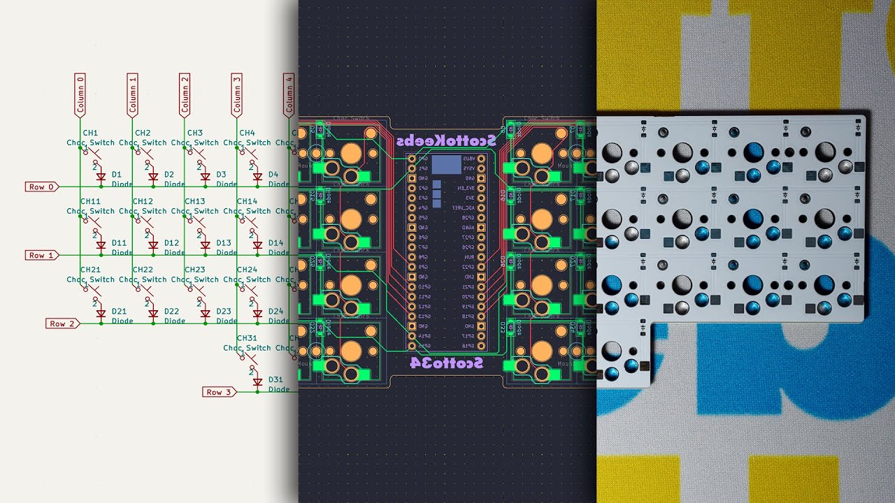
It looks like pad 5/VCC is on the middle-left, pad 2/GND is on the middle-right, and pad 6/data is on the upper-left of the footprint when I open the hillside46.kicad_pcb file in the KiCad PCB Editor, click on ‘View’, and check “Flip Board View”.
As a sanity check, given the info above: it looks like I could rotate that ESD chip 180 degrees (so that the ESD chip’s pin 1 is on the lower-right pad of the footprint) and have everything work, correct?
I really appreciate your offer, and I’d totally take you up on it if @SurvivorBobXYZ hadn’t already provided a reply above. Thank you so much for all of your help!
I do think this may have more to do with the fact that Beehaw, my current instance, recently made the decision to defederate with lemmy.world. Is that assumption correct?
deleted by creator


I’m not getting this, at least not yet.
Maybe it’s because I run Pi-hole; I know it filters out a TON of Roku’s telemetry and other traffic. Might be worth setting up Pi-hole on your network and see if stuff like that goes away?